Instruments

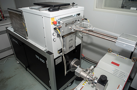
Plasma Enhanced Chemical Vapor Deposition System
The Plasma Enhanced Chemical Vapor Deposition system consists mainly of a plasma generator from Thermal Scientific, a tube furnace, and a 12L vacuum pump from Edwards. It is equipped with eight gas channels, with a working temperature range from room temperature to 1400K. This equipment is primarily used for the growth of graphene and two-dimensional transition metal chalcogenides.
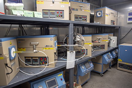
Tubular Furnace
We have seven dual-temperature zone tubular furnaces, model OTF-1200X-II, which can reach a maximum temperature of 1200°C. The two temperature zones are independently controlled by two temperature control systems based on PID algorithms, allowing for 30-segment programmed temperature control. By setting the control programs for the two temperature zones, a specific temperature gradient can be created inside the furnace. In addition, we also have one three-temperature zone tubular furnace, model OTF-1200X-III, which can independently control three temperature zones, with a maximum temperature of 1200°C. These furnaces can be used to grow nano-thin films or bulk single crystals using CVD or CVT methods.
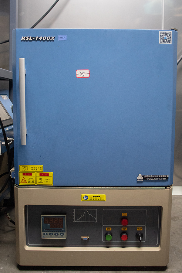
Muffle Furnace
We have one box furnace, model KSL-1400X-A3, with a maximum temperature of 1400°C. Additionally, we also have a LH30/13 muffle furnace manufactured by Nabertherm, which ensures good temperature uniformity with heating on five sides, and can reach up to 1300°C. These muffle furnaces are used to grow bulk single-crystal materials via flux methods.
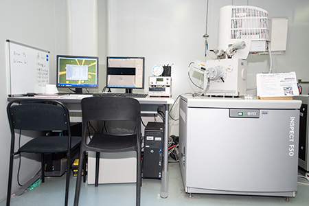
SEM-EBL System
The Scanning Electron Microscope (SEM) is used for characterizing the morphology of materials, with magnification that ranges from the optical microscope range to the nano-scale. Electron beam lithography, based on SEM, is a method for preparing semiconductor devices. It uses a focused scanning electron beam to expose custom patterns on a sample coated with an electron-sensitive resist. The primary advantage of electron beam lithography is the ability to create custom pattern devices as small as 10 nm in size.
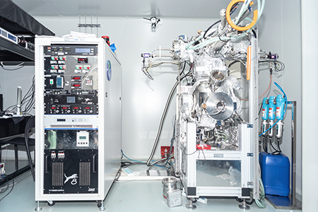
Electron Beam Evaporation and Magnetron Sputtering System
Electron beam evaporation is a mature and widely used coating method in vacuum deposition technology. Magnetron sputtering is a type of physical vapor deposition with advantages such as simple equipment, easy control, large coating area, and strong adhesion. This system integrates both electron beam evaporation and magnetron sputtering, and is equipped with an oil pump, molecular pump, and cryo-pump, achieving a maximum vacuum of 1E-8 Torr. The thin-film growth and metal electrode preparation functions of this system are essential for various sample preparation processes.
Atomic Layer Deposition System
Atomic Layer Deposition (ALD) is a technique used to deposit material on a substrate surface one atomic layer at a time. ALD is similar to ordinary chemical deposition, but during ALD, each new atomic layer reacts chemically with the previous layer, ensuring that only one atomic layer is deposited per reaction. ALD allows for precise control over the thickness, composition, and structure of the material, resulting in uniform and dense coatings. We primarily use this equipment for the growth of transistor dielectric layers and memristor switching layers.
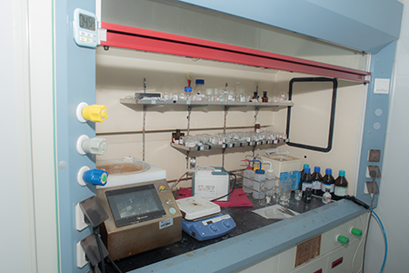
Chemical Operation Room
The chemical operation room provides a convenient and safe environment for nano-microfabrication. It is equipped with common instruments such as fume hoods, spin coater, hot plates, ultrasonic cleaners, stirrers, and refrigerators.
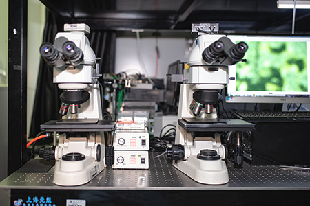
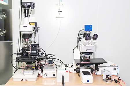
Optical Microscope
Four Nikon high-performance ECLIPSE Ci series upright research microscopes are used for sample observation and processing. The high brightness, environmentally friendly illumination lamp provides sufficient light intensity for phase contrast and simple polarized light observation. High-quality objectives deliver bright, high-contrast images. The microscope works with Nikon Digital Sight series cameras, making specimen imaging efficient and easy.
Atomic Force Microscope
The atomic force microscope has extremely high resolution and very low noise levels. With ScanAsyst and Peak Force Tapping modes, high-quality images can be obtained in minutes. Various modes and accessories help us obtain surface morphology information of samples and study their physical properties.

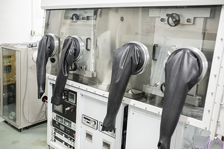
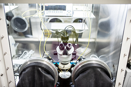
Multistage Combined Glovebox
Many quantum materials have enabled basic experimental research in quantum control. However, many of these quantum materials are highly unstable and susceptible to damage from oxygen and water in the air, which affects the performance stability of related micro-nano electronic components. The laboratory has four nitrogen gloveboxes and realizes multistage combination between gloveboxes, allowing electrical components made of materials to be processed in an oxygen- and water-free environment during various nanofabrication steps (such as sample stripping, heterojunction transfer, photoresist spin coating, electrode development, evaporation, wire bonding, and room-temperature electrical measurements).
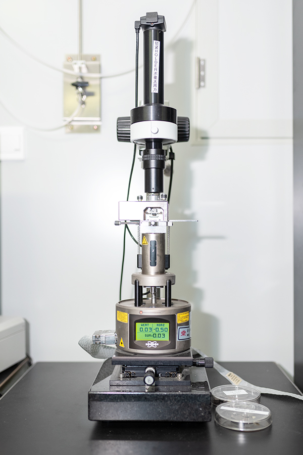
Two Sets of Controllable Transfer Equipment for 2D Materials (Inert/Atmosphere)
The interlayer van der Waals interaction of 2D materials allows them to stack and form artificial heterostructures without introducing defects or impurities. The transfer process requires adjusting the interaction between the organic thin film and different materials to achieve peeling, stacking, twisting, folding, flipping, and releasing of the 2D crystals on different substrates. The transfer stage is compatible with multiple transfer techniques and can be flexibly adjusted for different processes. By integrating stepper motors, precise control of spatial positioning with an accuracy of 0.1 μm can be achieved, avoiding interference and uncertainty caused by manual operations.
Inert Atmosphere Electron Beam Evaporator
Many quantum materials are highly unstable and easily damaged by oxygen and water in the air, which affects the structure of the material and the performance of the device. We have built an electron beam evaporation system combined with a nitrogen glovebox to prepare high melting point metal electrodes, such as Cr, Ti, Au, Pt, for the micro-nano electronic components of easily oxidized 2D materials and quantum materials, and conduct transport measurements at room temperature and low temperature in strong magnetic fields.

Inert Atmosphere Thermal Evaporator
Low melting point metals such as indium have been proven to greatly improve the contact resistance of 2D materials and some 3D topological materials. We have newly purchased a thermal evaporator operating in an inert atmosphere to prepare indium electrodes, thereby obtaining high-performance micro-nano electronic components. Additionally, due to indium's good flexibility, it can be used as the source and drain electrodes, as well as top-gate electrodes for flexible electronic components.
Inert Atmosphere Device Testing System
The room-temperature probe station, placed inside the nitrogen glovebox, allows for direct electrical measurements of devices in an inert environment, fully isolated from air/water vapor. This is crucial for rapid characterization and selection of easily oxidized 2D/quantum material electronic devices.

Wire Bonding Machines (2 sets, Inert/Atmosphere)
Wire bonding machines are used to connect integrated circuits (or other semiconductor devices) to semiconductor device packaging. They can also be used to connect integrated circuits to other types of electronic circuits (such as PCBs). Wire bonding is an efficient, cost-effective, and stable connection technology used in most semiconductor device packaging. Our laboratory has one wire bonding machine each for inert and atmospheric environments, mainly used to connect electronic devices made of 2D materials to chip carriers, which are the basis for all device measurements.
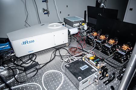
Raman Spectrometer
Raman spectroscopy is independent of the incident light frequency and is related only to the structure of the scattering sample itself. The spectral information depends on the changes in molecular vibration energy levels. Different chemical bonds or groups have characteristic molecular vibrations, so the corresponding Raman spectrum is also characteristic. Therefore, Raman spectroscopy can serve as a basis for qualitative analysis of molecular structures.
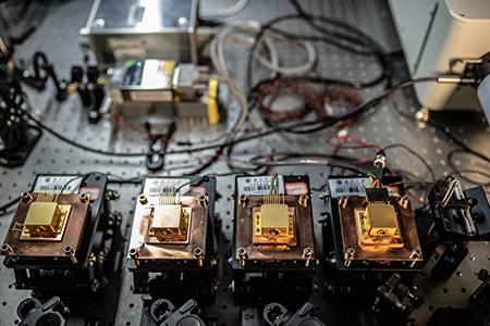
Mid-Infrared Laser
Mid-infrared lasers are used as light sources for infrared detection in optoelectronic devices, with four wavelengths of 4, 5, 8, and 10 μm.
Optical Cryostat
The Oxford Instruments low-temperature measurement system can cool to temperatures as low as 77K using liquid nitrogen. The instrument has an optical window at the top for light source illumination for optoelectronic testing. It also supports variable temperature Raman and PL measurements.

7T Magneto-Optical System
The Oxford Instruments SpectromagPT cryogenic magneto-optical system provides an integrated magnetic/optical/electrical measurement platform. The system has four optical windows at the bottom, and its base temperature is 1.5 K. The superconducting coil generates a 7T horizontal magnetic field.
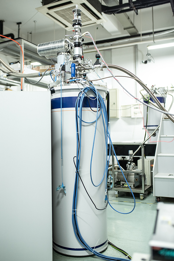
Oxford Instruments Low-Temperature Refrigerators (3 units)
The Teslatron PT system from Oxford Instruments integrates a superconducting magnet and a variable-temperature insert to provide low-temperature and high magnetic field measurement environments. The laboratory is equipped with three refrigerators, with maximum magnetic fields reaching 14T, 12T, and 8T, and temperature ranges from 1.5K to 300K. With the addition of helium-3 inserts and dilution refrigerator inserts, the lowest achievable temperatures are 250mK and 25mK, respectively. A rotating insert allows measurements in different magnetic field directions. This system serves as the foundation for low-temperature, high-field transport measurements of various samples.
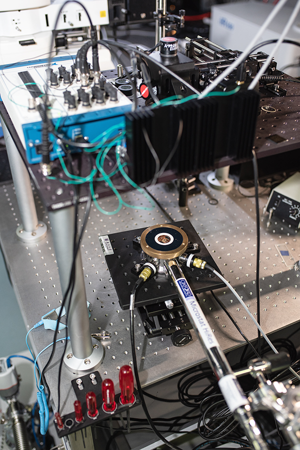
Weak Signal Testing Equipment
A variety of weak signal test source meters are essential for characterizing the transport properties of micro-nano devices. The laboratory currently possesses SR560 voltage amplifiers (9 units), SR570 current amplifiers (6 units), SR830 lock-in amplifiers (10 units), current sources (Keithley 6221, Yokogawa GS200) (3 units), and multi-functional voltage source meters (Keithley 2636, 2635, and 2400) (8 units).
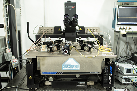
Cascade Summit Series Measurement Platforms
Utilizing PureLine and AttoGuard technologies, the Cascade Summit series measurement platforms provide a complete measurement range for testing equipment on 200mm and 150mm wafers. They support various applications, including RF/microwave, device characterization, wafer-level reliability, electrical testing, modeling, and yield improvement.
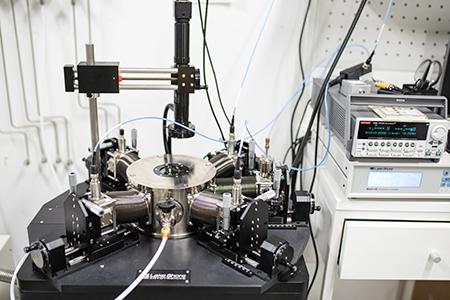
Array Test Probe Station
The array test platform is used for reading, writing, and matrix-vector multiplication of 1T1R arrays. The YB600 probe station is used to connect the on-chip memristor arrays with external testing equipment. The external testing equipment includes M9185A (DAC), M9101A, M9120A (matrix switches), M9216A (DAQ), and M9111A (SMU).
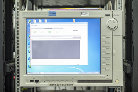
Semiconductor Device Analyzer
The Agilent B1500A Semiconductor Device Analyzer integrates multiple measurement and analysis functions into a single instrument, providing precise and rapid device characterization. It is the only multi-functional parameter analyzer capable of offering a wide range of device characterization functions with outstanding measurement reliability and repeatability. It can perform comprehensive measurements, from basic current-voltage (IV) and capacitance-voltage (CV) characterizations to advanced fast-pulse IV tests.
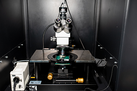
Lakeshore Variable-Temperature Probe Station
Research on semiconductor electronic devices requires analysis and testing of semiconductor samples at both low and high temperatures. The Lakeshore variable-temperature probe station uses a closed-loop helium refrigeration system, with a minimum temperature of 10K. Additionally, the high-temperature sample holder can reach a maximum temperature of 675K. The probe station also allows for electrical measurements of samples under illumination conditions.